In today’s embedded vision ecosystem, performance is no longer measured solely by resolution. Signal quality, frame stability, power efficiency, and system compatibility now define whether a camera module succeeds in industrial, medical, or intelligent automation applications. At the center of this evaluation is the image sensor itself.
Companies such as ELP, known for their experience in USB camera modules and embedded imaging solutions, leverage the Aptina MI5100 sensor to deliver reliable, application-ready camera systems for OEMs and system integrators worldwide.

Overview of the Aptina MI5100 Sensor Architecture
The Aptina MI5100 is a 1/2.5-inch CMOS image sensor with a native resolution of 2592 × 1944 pixels (5MP). Designed for embedded and industrial imaging rather than consumer photography, it prioritizes signal integrity, controllability, and system-level stability.
Key architectural characteristics include:
Active-pixel CMOS design
High signal-to-noise ratio
Rolling shutter operation
Programmable exposure and gain control
Parallel and serial data output support
This architecture makes the MI5100 particularly suitable for machine vision, document scanning, medical imaging, and industrial inspection.
Image Quality Advantages in Practical Applications
High Resolution with Controlled Noise
The 5MP resolution of the Aptina MI5100 sensor provides sufficient spatial detail for inspection and analysis tasks without generating excessive data load. Its pixel design supports low read noise, enabling clearer images in controlled and moderately low-light environments.
Accurate Color Reproduction
Thanks to optimized color filter arrays and on-chip processing, the MI5100 delivers consistent color fidelity, an essential requirement for applications such as medical diagnostics, laboratory imaging, and quality inspection.
Flexible Exposure Control
The sensor supports programmable exposure windows and gain settings, allowing system designers to fine-tune image capture based on lighting conditions and motion characteristics. This flexibility improves usability across varied deployment scenarios.
Integration Benefits for Embedded Camera Modules
System Compatibility
The Aptina MI5100 sensor integrates smoothly with common image signal processors (ISPs) and USB bridge chips, simplifying camera module development. This compatibility reduces firmware complexity and accelerates product deployment.
Power and Thermal Efficiency
Compared with higher-resolution sensors, the MI5100 maintains reasonable power consumption, helping designers manage thermal constraints in compact enclosures. This makes it suitable for continuous-operation systems.
Long-Term Availability
In industrial and embedded markets, component lifecycle stability is critical. The MI5100 has been widely adopted, making it easier for manufacturers like ELP to provide consistent supply and long-term support for camera modules built around this sensor.
Applications That Benefit Most from the Aptina MI5100 Sensor
Industrial Machine Vision
For inspection tasks such as surface defect detection, dimensional measurement, and barcode recognition, the MI5100 offers a balance between resolution and processing efficiency. Its stable output supports real-time analysis in automated systems.
Medical and Laboratory Imaging
In medical carts, diagnostic devices, and lab instruments, image clarity and repeatability matter more than extreme resolution. The Aptina MI5100 sensor delivers predictable, calibrated output, supporting professional imaging requirements.
Document and Object Scanning
High pixel density and uniform illumination response make the MI5100 suitable for document scanners, OCR systems, and archival imaging solutions.
Embedded AI and Vision Systems
When paired with edge processors, MI5100-based cameras provide sufficient visual detail for AI-assisted recognition and classification, without overwhelming system bandwidth.
Why Camera Module Design Matters as Much as the Sensor
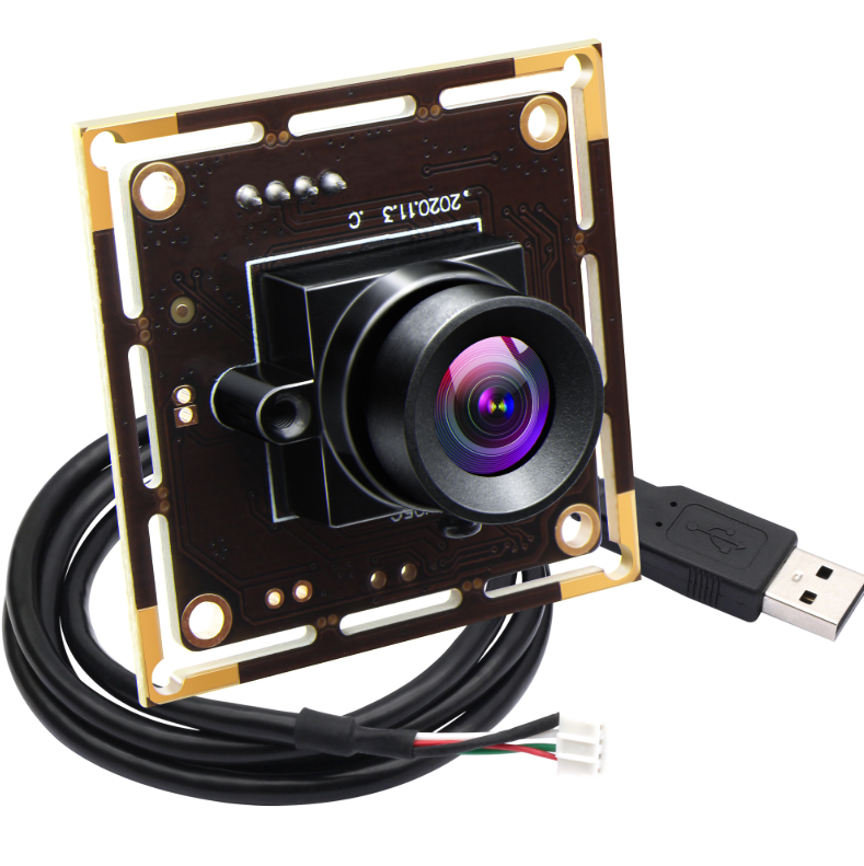
While the sensor is central, lens quality, PCB layout, shielding, and firmware tuning all influence final image performance. ELP specializes in integrating the Aptina MI5100 sensor into well-engineered camera modules that address:
Optical alignment accuracy
EMI and signal stability
USB data integrity
Mechanical reliability
This holistic design approach ensures the sensor’s capabilities are fully realized in real-world deployments.
Comparing the Aptina MI5100 to Newer Sensors
Although newer sensors offer higher resolutions, they often introduce:
Increased power consumption
Higher processing requirements
Greater system cost
For many industrial and embedded applications, the MI5100 remains a cost-effective, proven solution that meets performance needs without unnecessary complexity. Its maturity is a strategic advantage rather than a limitation.
Conclusion: Proven Sensor Technology with Practical Value
The Aptina MI5100 sensor represents a mature, dependable imaging solution that balances resolution, image quality, and system efficiency. When integrated into professionally designed camera modules, it delivers consistent performance across demanding applications.
Through careful engineering, optical matching, and firmware optimization, ELP enables OEMs and integrators to harness the full potential of the MI5100 sensor—transforming reliable silicon into practical, deployable vision solutions.


